


Quartz crystal application notes
1. Cutting angles and vibration mode
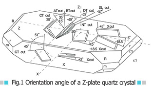
Cutting angles differ depending upon the applications. (oscillation frequencies and electrical characteristics)Fig 1. shows main cutting angles and Table shows vibration modes, frequence ranges and capacitance ratio. (typical values) Taking the most popular AT-cut crystal wafer for example, it is in a plane which makes an angle of 35°15′to the Z axis and the wafer thickness is approximately 0.16mm in the case of 10MHz fundamental-mode thickness-shear vibration.
| Mode of vibration | Orientation angle | Frequency range (KHz) |
Frequency (KHz) |
Capacitance ratio(approx) |
|
|---|---|---|---|---|---|
| Tuning fork | 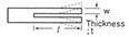 |
+2°× | 24 ~ 25 | 770 × |
450 |
| Flexure | 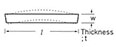 |
XY XY |
1 ~ 21 21 ~ 85 |
5700 ×
 5000 × |
600 900 |
| Extensional | 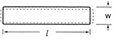 |
+5°× -18.5°× |
50 ~ 200 60 ~ 650 |
2730 ×
 2550 × |
140 140 |
| Face shear | 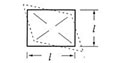 |
DT CT SL |
84 ~ 300 250 ~ 1150 300 ~ 1150 |
2080 ×
3080×
(460 × ) |
450 450 450 |
| Thickness shear |  |
AT fundamental AT N-th overtone BT fundamenta |
800 ~ 30000 3000 ~ 75000 2000 ~ 38000 |
1670 ×
 1670×
 2560 × ) |
300 ~ 450 (2500) 650 |
2. Frequency?Temperature Characteristics
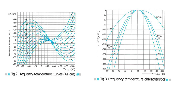
Fig. 2 shows the frequency-temperature characteristics for a thickness-shear mode AT-cut with the angle of cut as a parameter. Since the AT-cut frequency-temperature characterictic is equivalent to an equation of the third degree, it displays excellent frequency stability over a wide temperature range. Fig. 3 shows the frequency-temperature characteristics of the mode of vibration other than AT-cut. All vibration modes show an equation of the second degree. Therefore, when the operating temperature range is wide, the frequency change is much larger than that of the AT-cut. Therefore, the AT-cut is most widely used.
3. Frequency?Temperature Characteristics
4. Description of terminology
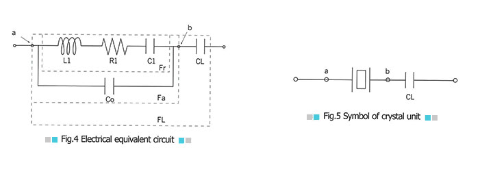
- Fo = Nominal Frequency
- Fr = Fs = Series Resonant Frequency
- Fa = Fp = Antiresonant Frequency
- FL = Load Resonant Frequency
- C1 = Motional Capacitance
- L1 = Motional Inductance
- R1 = Equivalent Series Resistance
- CO = Shunt Capacitance
- CL = Load Capacitance
- RL = Load Resonance Resistance
- ΔF = dF = Frequency change
- ΔF/Fo = Frequency stability
- γ = Capacitance Ratio
- Q = Quality Factor
- M = Figure of Merit
- LO = Load Resonance Frequency Offste (Fr vs. FL)
- PR = Pulling Range
- S = TS = Pulling Sensitivity
- Ct = Max. Load Capacitance
- DL = P = Drive Level
5. Useful formulas for crystal unit
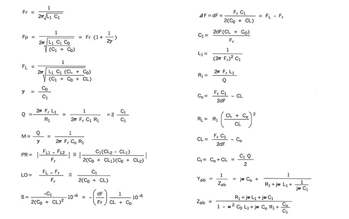
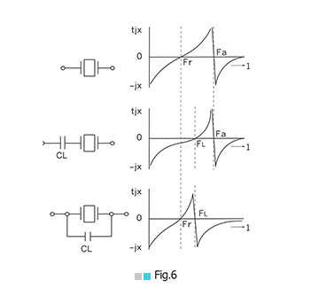
6. Crystal unit and load capacitance
The load capacitance CL is a factor for determining the “conditions” of a crystal unit when used in the oscillation circuit. In an ordinary oscillation circuit, the crystal unit is used in a range where it functions as an inductive reactance. In such usage, the oscillation circuit operates as a capacitive reactance. In other words, when the oscillation circuit is seen from both terminals of the crystal unit, this oscillation circuit can be expressed as a series circuit of negative resistance and capacitance. At that time this capacitance is called the load capacitance.
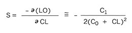
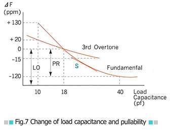
7. Change of load capacitance and pullability
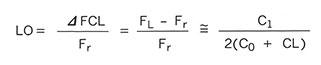
For many applications there are requirements to pull the crystal frequency by using a load reactive element. This may be necessary in order to trim out the manufacturing tolerance or in phase locked loop and frequency modulation applications. In most applications the load reactive element in capacitive and therefore only this case is now considered. The fractional difference in frequency between the load resonance frequency (FL) and the resonance frequency(Fr) is known as the load resonance frequency offset(LO).
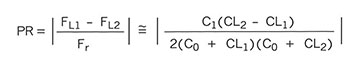
In many applications a variable capacitor(trimmer) is used as the load reactive element to adjust the frequency. The fractional frequency range available between specified values of this load reactive element is called the pulling range(PR) and it can be calculated by using the following formula :
A useful parameter to the design engineer is the pulling sensitivity(S) at a specified value of load capacitance. It is defined as the incremental fractional frequency change for an incremental change in the load capacitance. It is normally expressed in 10-6/pF and can be calculated from the formula :
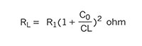
The equivalent circuit of the crystal has one other important parameter : this is R1, the motional resistance. This parameter controls the Q of the crystal unit and will define the level of oscillation in any maintaining circuit. The load resonance resistance for a given crystal unit depends upon the load capacitance with which that unit is intended to operate the crystal manufacturer has equipment to measure these quantities. The frequency of oscillation is the same in either a series or parallel connection of the load capacitnce. If the external capacitance is designed the load resonance resistance(RL) may be calculated as follows :
8. Illustrated flow chart for quartz crystal unit
| Process | Process Drawing | Description of process |
|---|---|---|
| Slicing | 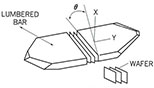 |
With the r-surface of a lumbered crystal used as the reference, wafer-shaped pieces are cut out at the prescribed angle. |
| Measurement of angle | 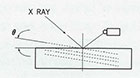 |
To confirm that the crystal is cut at the prescribed angle, the angle is measured by means of an X-ray angle checker. |
| An outward form processing |  |
To prevent joining with other vibration modes and from being influenced by sub-vibrations, the external shape is properly corrected by profiling. |
| Lapping | 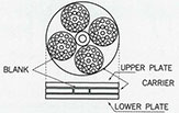 |
Since frequency of AT-cut crystals is determined by the thickness of the crystal piece, the thickness of the crystal pieces is made uniform by means of a surface lapping machine to raise the surface accuracy. |
| Etching & cleanin | 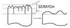 |
After removing the worked laver produced by precision lapping and beveling by etching, cleaning is carried out |
| Electrode metal evaporation |  |
The electrode used for applying a electric field to the crystal piece is formed by vacuum metal evaporation (Ag. etc.) on surface of the crystal piece. |
| Fine frequency adjustment | 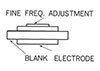 |
Final fine adjustment of the frequency is carried out by vacuum metal evaporation or ion gun etching while letting the crystal oscillate. |
| Assembly | 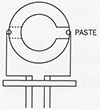 |
The crystal piece is secured to the base by such means as Agpaste. |
| Sealing | 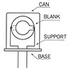 |
To suppress aging of the crystal piece, the inside of the holder is first made vacuum, or filled with such inactive gas N2 and then sealed with a cap. |
| Inspection |  |
The crystal pieces are inspected for their specifications including frequency deviation, frequency vs temperature characteristics, equivalent resistance, hermetic of seal and insulating properties. |
9. Crystal holders
- Solder Seal : This method is cost effective and accepted for military and commercial applications. (Mil-C-3098) Nickel-Silver cans and bases are soldered together with a tin-lead alloy.
- Resistance Weld : Resistance welded enclosures are sealed together by melting the metal for a very short time with a large predeter mined electrical pulse, thus welding the crystal cover to the base. No fluxes are used in this process. The resistance-weld method has the advantages of approaching the long term stability of the coldweld method. Typical aging per year for resistance weld is <5ppm.
- Coldweld : In the coldweld method a nickel plated copper can and base are sealed together under a concentrated high pressure bonding technique. The enclosure is evacuated using a cryogenic vacuum and backfilled with a mixture of helium and nitrogen. The coldweld method is exclusively used when long term stability is required (low aging characteristics). Typical aging per year for coldweld is <3ppm. Coldweld sealed crystals are slightly higher cost.
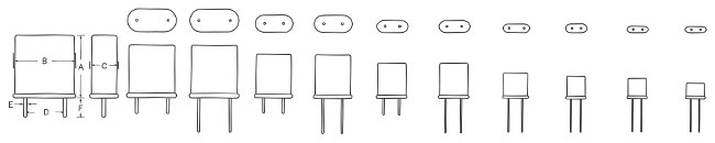
| Solder seal | HC - 6 | HC - 33 | HC - 32 | HC - 32/WL | HC - 25 | HC - 18 | HC - 44 | ||||
|---|---|---|---|---|---|---|---|---|---|---|---|
| Resistance weld | HC - 48 | HC - 51 | HC - 50 | HC - 49 | UM - 2 | UM-1/SLIM | UM-5/SLIM | ||||
| Cold weld | HC - 36 | HC - 47 | HC - 46 | HC - 46/WL | HC - 42 | HC - 43 | |||||
| A | 19.69 | 19.69 | 16.26 | 16.26 | 13.46 | 13.46 | 9.50 | 8.00 | 7.62 | 5.79 | |
| B | 19.23 | 19.23 | 14.40 | 14.40 | 11.05 | 11.05 | 9.40 | 7.80 | 7.49 | 7.80 | |
| C | 8.94 | 8.94 | 6.02 | 6.02 | 4.65 | 4.65 | 3.51 | 3.10 / 2.4 | 2.59 | 3.10 / 2.4 | |
| D | 12.40 | 12.40 | 6.99 | 6.99 | 4.88 | 4.88 | 4.88 | 3.76 | 2.84 | 3.76 | ±0.2 |
| E | 1.27 | 1.27 | 1.02 | 1.02 | 1.02 | 0.43 | 0.41 | 0.36 | 0.43 | 0.36 | ±0.05 |
| F | 6.05 | *12.7 Min | 6.05 | *12.7 Min | 6.05 | *12.7 Min | *12.7 Min | *12.7 Min | *12.7 Min | *12.7 Min |
* Flexible wire leads
10. Reflow Soldering
The figure below shows the standards for reflow soldering temperature profiles of surface-mount type crystal units.
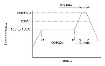
● Soldering conditions
Peak-temperature: 260±5 °C Max. 10 seconds
Heating conditions: Min 230 °C 30 ±10 seconds
Warm-up rate: Max. 3 °C/second
Cool-down rate: Max. 6 °C/second
Preheating conditions: 150 to 180 °C 90 ±30 seconds
Precautions
Never use these products under any conditions that exceed the following limits; such use may cause the product’s characteristics to deteriorate or the product may break.
Heat Resistance of SMD Crystal Products
[Reflow Soldering Heat Resistance]
Peak-temperature: 265 °C, 10 sec.
Heating conditions: Min. 230 °C, 40 sec.
Warm-up rate: 3 °C/second
Cool-down rate: 6 °C/second
Preheating conditions: 150 to 180 °C, 120 seconds
Number of reflow passes: 2
[Manual Soldering Heat Resistance]
Use condition: Apply 400 °C soldering iron to product terminal electrode for 4 seconds.
Number of applications: 2